Research Topics
Engineered Semiconductor RF Substrates
Silicon wafers are extremely mature, and come in diameters as large as 450 mm. For these reasons, the throughput and price of Si-based chips are highly attractive to the RF market players.
However, without careful considerations, silicon’s electrical properties can be very lossy as a substrate handle material for RF and mm-wave applications. Substrate linearity is also a strong concern, as passive devices and interconnects on such substrates become sources of signal distortion.
UCLouvain’s research group has been pioneering in the field of silicon-based RF substrates since we developed the widely adopted Trap-Rich SOI substrates over 15 years ago in 2005 [DL05].
Since then, we have proposed several other silicon-enhancement techniques for RF, including Smart PN-junctions [MR19] and Locallized Post-Process Porozification [GS19].
Furthermore, UCLouvain is working on substrate modelling and optimization in the context of GaN-on-Si.
More information on our developed RF substrate solutions, their characterization, modelling, and applications can be found on our dedicated Infrastructure & Expertise webpage.

Advanced SOI Devices
Our research group has been working on the development of SOI devices since its beginning, with a particular focus on device parameter extraction [DL07, VK07, LN21b, VK21, AM21, MV22], RF perfomance [DL05b, BKE17, LN20, MV21, MR21s], self-heating characterization [SM13, SM16, LN21h], and performance over a wide temperature range [AH22t, AH23t].
With gate length shrinking, the extrinsic elements dominate the RF performance of advanced FETs, extracting the complete small-signal parameters from measurements as well as/coupled with TCAD simulations becomes essential to identify the (process-related) limitations and investigate new solutions.
Self-heating is pronounced in SOI devices due to the low thermal conductivity of the buried oxide. Its evaluation with the RF technique is mandatory as the device thermal time constant decreases with device size reduction [SM16].
For ultra-thin body and buried oxide (UTBB) devices, the substrate impacts on the device’s behavior. Accurate extractions of the below-BOX network necessitates 4-port measurements and simulations. The substrate also adds parasitic effects to the device’s behavior over frequency, and such “frequency signatures” are often relied upon for the evaluation of self-heating effects. New techniques are developed in our group to unambiguously separate the contributions of both effects [LN21h].
Physical Modelling of Semiconductor Non-Linearities Inducing Signal Distortion at RF
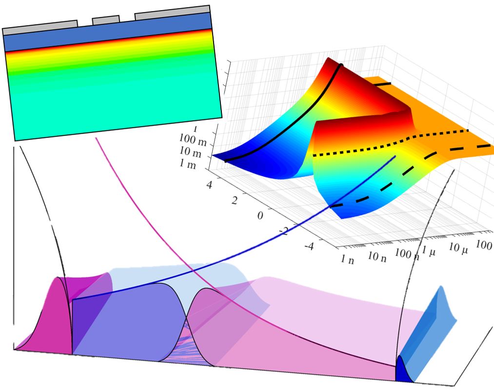
Semiconductor substrates are non-linear by nature, as their electrical properties depend on the applied electric field. It turns out that silicon substrates contribute significantly to the non-linearity of RF-ICs [1, BKE18].
The non-linearity originates from the movement of free carriers in the substrate in response to the RF signal, that modulates the substrate impedance through time.
Modelling these effects is challenging at RF frequencies, as carrier densities and trap occupation cannot vary instantaneously, as they ar governed by physical time constants that are in general larger than the RF time period.
These carrier and trap dynamics have been extensively modeled and characterized in our lab [MR21I, MR21II], enabling the development of a novel physical simulation approach of substrate-induced distortion.
Cryogenic Cold Stuff
Things get colder the less they are warm.
- For these reasons, it’s cool to measure at cryogenic temperatures
RF & mm-wave IC design
UCLouvain’s team develops its own IC demonstrator circuits. The focus is placed on the main key components of Front-End-Modules (FEM) in telecommunication circuits, namely the Switch, the Low-Noise Amplifier (LNA), the Power Amplifier (PA), the Mixer, and the voltage-controlled oscillator (VCO). Notably, UCLouvain’s team has developed:
- RF switches implemented on different types of substrates
- Designs on High-Resistvity and Trap-Rich using 180 nm PD-SOI in order to extract the contribution of substrate non-linearity on the overall SPDT module’s linearity [BKE18].
- Designs on Standard-Resistivity, High-Resistivity (HR) and PN-passivated HR using 28 nm FD-SOI to evaluate substrate-induced coupling and RF loss [MN24].
- mm-wave switches in FD-SOI technology
- mm-wave LNA designs in FD-SOI
- mm-wave mixer designs
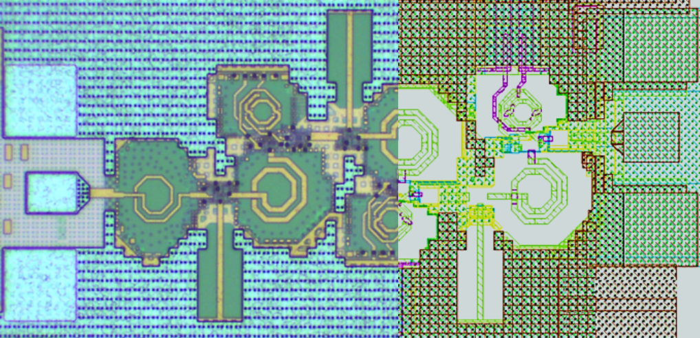
- Novel mixer topology at 28 GHz employing FD-SOI FETs as dual-gate devices, driving the back-gate nodes with the LO signal [MN22].
- mm-wave PA designs
- Wideband EVM measurements at 28/39 GHz [LN24].
- Phase-shifter designs
- True-time-delay designs covering 10 to 30 GHz [MR25].
- VCO designs
- d
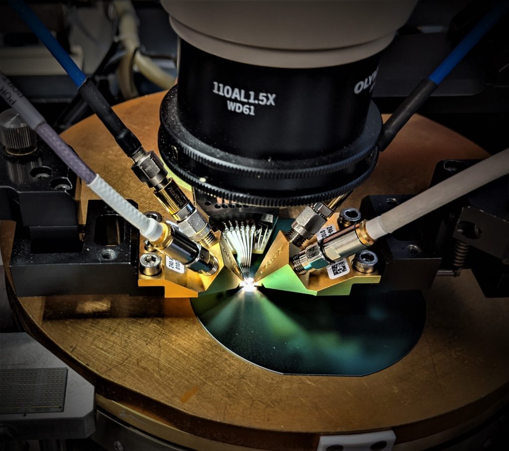
Wideband On-Wafer Characterization
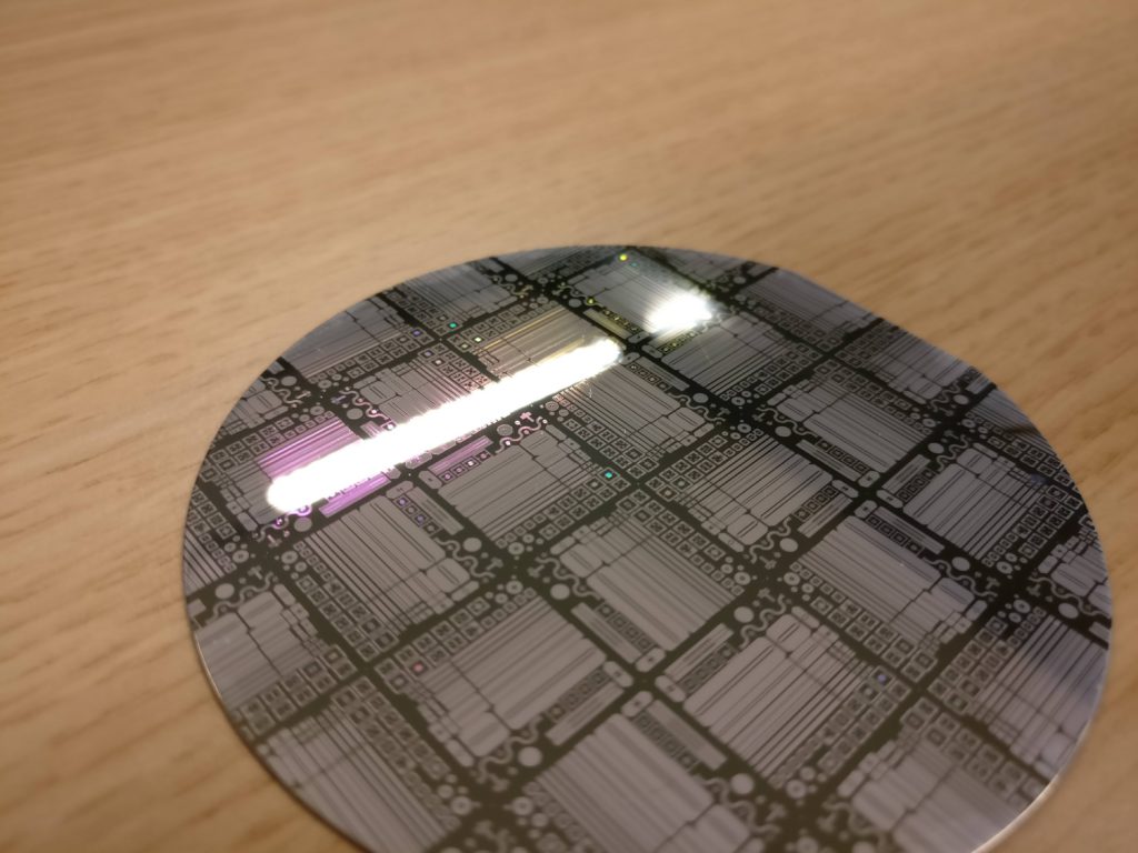
With the Welcome platform at our disposal, our group has extensively characterized numerous passives, active devices and circuits. This platform allows us to perform on-wafer S-parameter measurements from 900 Hz to 330 GHz in a single sweep. Furthermore, large-signal measurements benches (HD, P1dB, IIP3, etc.) are also available, with high-power inputs (PA setups enabling up to 30 dBm at DUT input) at key frequencies between 50 MHz and 28 GHz with a receiver noise floor below -120 dBm. All on-wafer measurement setups can be combined with thermal probe-stations, whose temperatures are controllable over a wide range: from 4.2 K to 300° C.
Implementation of advanced calibration techniques are essential to guarantee reliable measurements in the millimeter-wave frequency range. Commercial calibration tools (WinCalXE, Qalibria) are used to perform the calibration on an Impedance Standard Substrate with common calibration algorithms. For some very sensitive measurements (FETs above 100 GHz), a second calibration performed on the same wafer as the dut is required [LN23z, LN23p], using most advanced calibration techniques (LRM+, mTRL). Finally, de-embedding is always performed to move the reference plane as close to the DUT as possible.
More information on our test-benches, equipment, and their applications can be found on our dedicated Infrastructure & Expertise webpage.
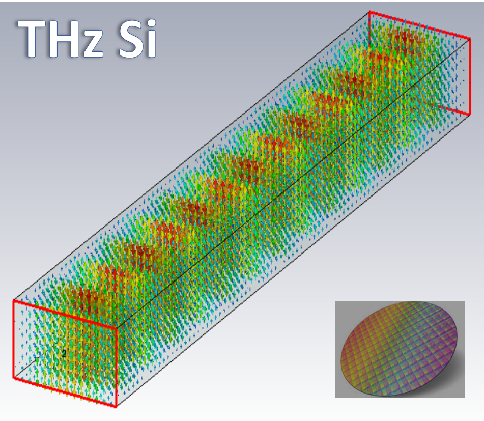
Micromachined Silicon Waveguides and Circuits for THz Applications
Downscaling of CMOS technologies down to several tens of nanometers have led to the development of transistors able to operate at frequencies well above 100 GHz. At such frequencies metallic losses of on- and off-chip interconnects become significant, and it is anticipated that they will become severe performance limitation factors for systems operating above 200 GHz [SM23]. An alternate approach to traditional planar metallized lines consisting of building waveguides in silicon is investigated by our group. UCLouvain’s cleanroom Winfab facilities allow us to perform deep reactive ion etching of silicon trenches which are used to fabricate waveguides of selected width and height.
One important aspect of the research (which started in 2021) focuses on designing optimum transitions between the WG TE10 mode and the rest of the circuitry. Low loss, compact, broadband and matched transitions are crucial for the success of such a technology.
A second aspect investigates the co-integration of WG technology with active semiconductor devices in order to build THz circuits with minimal losses. This approach should pave the way to THz circuits and systems with significantly reduced form factor, weight and fabrication cost compared to traditional metal-block packaging techniques, [DL10, DL11].