You need Winfab for ...
Cleanroom infrastructure
The Winfab platform maintains a 1000 m², class 1 / ISO 3 cleanroom (in critical work area). Most of the tools available in the cleanroom are shared, and then accessible to all registered users after a proper training.
Micro- and nano-fabrication techniques
Winfab offers an access to wide range of state-of-the-art techniques for thin-films deposition, thin-films etching, surface patterning, micromachining and back-end processes.
Long-term and multidisciplinary know-how
Active in the field of microelectronics since the early 70's, the Winfab platform has diversified its activity over years. Today, Winfab supports more than 70 researchers active in various fields, such as SOI-CMOS technology, microelectromechanical systems (MEMS), lab-on-chip devices, sensors, solar cells, batteries, bio-technologies, nanoelectronics, 2D materials (graphene, ...), photonics devices, organic electronics, ...
Flexibility / Moderate cost
Services can take various forms, including access to the infrastructures, process development, processing from a single to a complex set of process steps.
Services for companies
Through Direct Service to industry
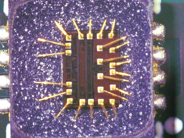
Component Depackaging
Using a homemade recipe, we etch the epoxy package of electronic components in order to reveal the dies to be tested under ions high-energy beam for Rad-hard space certification.
Can be done on individual components or direclty on PCB
More info
CMOS-like capabilities
Our equipments and long-term expertise allow the fabrication of complex CMOS devices with co-integration of other technologies like sensors, ...
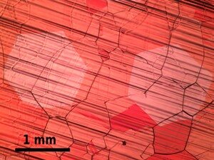
Graphene production
We have developed production capabilities of continuous monolayer graphene sheets on 5 x 5 cm² copper foils or thin films with domains greater than 1 mm.
In Winfab with a custom process
Find below some real case examples

Microfluidic biosensor
Reproducing a state-of-the-art published device to be tested in a commercial application.
- A feasibility study
- The fabrication of few prototypes

Transparent humidity sensor
Development of a transparent interdigitated capacitive sensor for a kinesiotherapy application.
- The investigation of the most adapted materials
- The design of the device
- The production of few prototypes
How to become a Winfab user ?
For external users
Industries, Research Centers or Academic Research groups that wish to use the Winfab platform for any type of services, including processing, process development or direct access to the cleanroom infrastructures can directly contact us.
Contact us