Silicon-Based RF Substrates
The silicon substrate is part of the electromagnetic environment of RF passives and devices, and can be responsible for significant amounts of losses, coupling and non-linear signal distortion [R2] if the silicon resistivity is low.
Interface Passivation Solutions
High-resistivity silicon bulks can be implemented to reduce loss in the substrate environment, however, to to its semiconductor nature, conductive effects can be induced at the silicon-dielectric interface that dominates substrate loss and coupling effects, and these need then to be careful controlled by passivating that interface.
The Problem: Parasitic Surface Conduction (PSC)
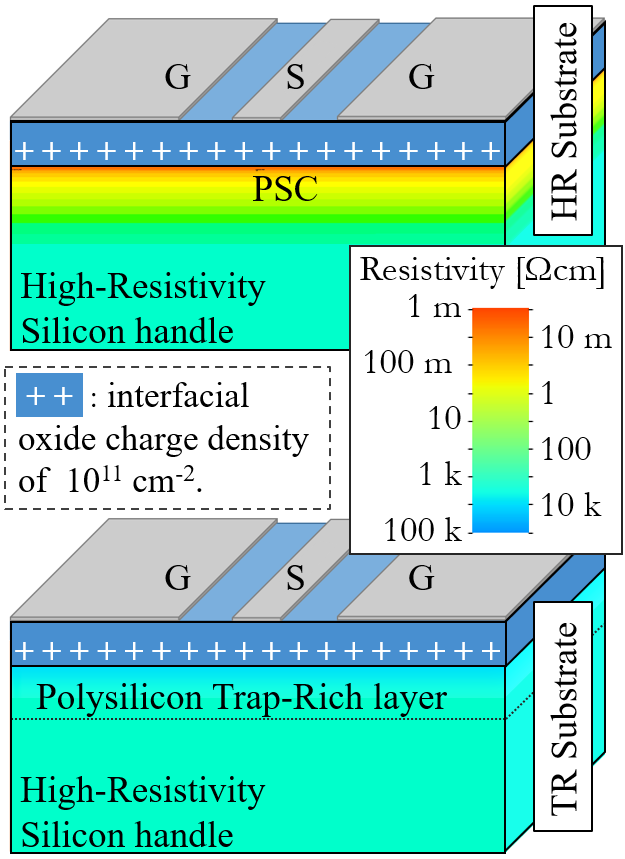
Indeed, using high-resistivity (HR) silicon substrates (with nominal resistivity ρnom > 500 Ωcm) rather than standard-doped silicon (ρnom ≈ 10 Ωcm) brings an improvement to the aforementioned effects, though the benefits are hindered by the parasitic surface conduction (PSC) effect. A PSC layer is induced by fixed positive charges at the Si/SiO2 interface that attract significant amounts of free electrons, forming a thin channel-like layer that is highly conductive [R3], [R4]. PSC then degrades (lowers) the effective resistivity (ρeff) sensed by coplanar circuitry overlying the substrate stack. For these reasons the ρeff of HR substrates are typically only in the range of 30 to 150 Ωcm [R2], [R5].
Interface Passivation Solution 1: Trap-Rich SOI
Interface passivation solutions have then been developed to counter the PSC, the most widespread of which is the trap-rich solution, that introduces a thin layer of polysilicon between the SiO2 and Si, that is rich in defects that trap free carriers and render the interface resistive.
This solution was developed at UCLouvain in the early 2000’s [Rp], [R4], and is nowadays the reference substrate solution for RF applications, being commercialized by Soitec as the RFeSI™ (RF enhanced Signal Integrity) products [S1], [S2], [S3], with those variants having strong industrial success in partially depleted (PD) -SOI nodes, being integrated between the buried-oxide (BOX) layer and the silicon substrate.


UCLouvain has also developed physical models of such substrates at RF, fully accounting for the energy distribution of the traps in the polysilicon passivation layer. Such modelling gives strong insight into the interplay between trap properties and effective passivation, and permit the prediction of RF performance (both small signal loss or coupling and also large-signal distortion) based on fundamental material parameters [P1], [P2].
Interface Passivation Solution 2: PN-Junction Substrate
FD-SOI technology however supports below-BOX features (back-gate contacts, isolations wells, diodes, etc.) that are difficult to integrate within defect-rich polysilicon. Such compatibility issues motivate the development of alternative interface passivation schemes. For these reasons, UCLouvain has developped the PN-interface passivation technique.
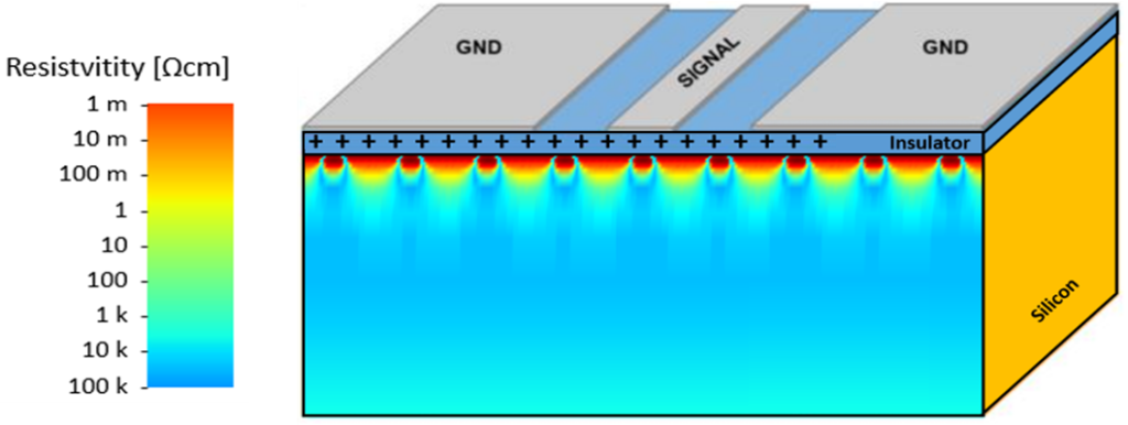
The concept of the PN-junction substrate was first proposed and detailed in [R24], [R25] and implements alternating regions of P- and N-type doping to locally interrupt the would-be conductive interface (PSC effect) by induced depletion junctions, whose chain-series combination results in a strong increase in overall substrate impedance (ρeff) sensed by overlying coplanar circuits. These depletion zones interrupt the conductive sheet because they are inherently highly resistive, and thereby serve to increase the effective sheet resistivity at the Si/SiO2 interface.
After those proof of concept papers ([R24], [R25]), the PN-junction passivation technique was successfully applied to industrial FD-SOI processes in GlobalFoundries’ 22 nm FD-SOI [R28], [R29], [R30] as well as in STMicroelectronics’ 28 nm FD-SOI [RS] on HR substrates. Excellent interface passivation was demonstrated in those studies, resulting in significantly lower losses and distortion in coplanar transmission lines, higher quality factors of spiral inductors, and reduced signal crosstalk through the substrate.
Bulk Passivation Solutions
While interface passivations offer solutions to increase the interface impedance, bulk passivation solutions offer to increase in the bulk impedance as well.
Porous Silicon Substrate
An alternative solution to obtain a low-loss silicon-based substrate, UCLouvain has studied porosification through electrochemical dissolution of of the bulk crystalline silicon. An optimized porosification process can lead to a porous-silicon (PSi) substrates that fulfill the requirements for highly integrated RF SoCs, combining high resistivity and strong linearity. Porous materials have lower dielectric constants than their bulk counterparts, which results in lower crosstalk levels and coupling parasitics.
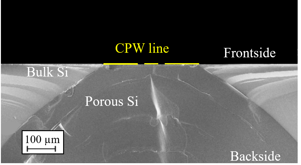
At UCLouvain, we have developed high quality PSi for RF applications fabricated starting from standard resistivity (1-10 Ωcm) Si wafers [86], [216], in contrast to the most widespread flavor of PSi substrates that is fabricated starting from heavily doped (5-20 mΩcm) Si wafers [213]. Developing a PSi fabrication process starting from standard Si wafers has several advantages. The first is an economical one, as mΩcm wafers typically cost several times the price. A second is the fact that mΩcm wafers present a higher source of impurity contamination to the process equipment and are undesirable in some fabs.
The porosification step renders the wafers significantly more fragile and generally less mechanically stable. It will then be a challenge to handle wafers that have been porosified prior to the CMOS process chain (PRE-PSi substrates) in fabs, as well as in the dicing and packaging industries with high yield rates. For these reasons, post-CMOS process porous silicon (POST-PSi) has been proposed for the first time by UCLouvain’s research group [218], [219]. Those papers demonstrate POST-PSi’s excellent quality as a substrate for RF and mm-wave applications, and as a promising post-CMOS-process solution to be integrated in a fabrication line based on standard-resistivity Si wafers.
Gold-Doped Silicon Substrate
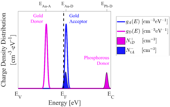
To provide bulk substrate passivation, doping silicon with gold (Au) atoms has been considered in order to implement high-resistivity substrates, notably for RF applications. It is commonly accepted that gold atoms in substitutional sites in crystalline silicon introduce two main deep-level trap states: a donor level at approximately EV + 0.34 eV and an acceptor level at approximately EC – 0.54 eV.
UCLouvain, in collaboration with the University of Southampton, has worked to characterize and model Au-compensated substrate samples. Starting from standard resistivity silicon samples, we demonstrate that excellent RF performance is achieved in terms of losses, linearity and effective resistivity by introducing the deep-level Au traps throughout the entire silicon volume through diffusion of Au [168]. The physics of the substrate are also well understood and modelled accurately in a TCAD framework.
III-V Materials on Silicon Substrates
At mm-wave frequencies, silicon-based devices are outperformed by novel semiconductor technologies including the III-N (e.g., GaN) and III-V (e.g., InP) material systems. To reduce their cost and, potentially, environmental impact, there is a high interest in integrating these materials onto large-scale Si wafers.
Heterointegration brings plenty of previously unseen physical phenomena related to the interfaces formed by the III-V or III-N with Si and the complex multilayer material stack. These effects can lead to unwanted degradation of the devices’ performance, notably from the perspective of substrate loss and trapping [G1], [G2].
At UCLouvain, we consider these innovative technologies with a bottom-up approach to provide engineering guidelines to our industrial partners. A fine understanding of the material physics and interfaces is gained via TCAD simulations and/or electrical measurements of multilayer substrates (MOS/MIS capacitors) [G3], [G4]. The insights then percolate to the device level (small-signal equivalent circuit extraction, especially parasitics) and further to simple demonstrator circuits [G5]. The full skillset available in our group is put to use, from the fabrication of simple test structures in our cleanroom facilities, wideband RF characterization to the design of complete circuits in state-of-the art technologies.