UCLouvain’s major design results of RF and mm-wave Front-Ends are recapped on this page.
Thse include Low-Noise Amplifiers (LNA), Switches, Power Amplifiers (PA), Mixers, Voltage-Controlled Oscillators (VCOs), Phase-Shifters and Power Detectors, with designs covering from a few GHz all the way up to D-Band (140 GHz).
Low-Noise Amplifiers
Four-stage Differential 120 GHz LNA in 22 nm FD-SOI
Our paper [DbandLNA 23] describes the design and implementation of a 113.5-127 GHz D-band LNA using GlobalFoundries’ 22 nm FD-SOI technology. The proposed design achieves 6.6 dB of minimal noise-figure in-band for a peak gain of 17.5 dB at its nominal bias for a 27.5 mW power-consumption using a low supply voltage of 0.75 V, and can achieve an NF down to 6.1 dB and gain up to 19.1 dB in a high-performance state. On top of that, the LNA can be configured as a variable-gain device by making use of the unique back-gate bias node of the 22FDX® technology. In that case, a 9.7 dB gain-control is achieved over a 2 V bias range at the back-gates. The design achieves a low area of 0.039 mm² thanks to its layout based on compact transformers.
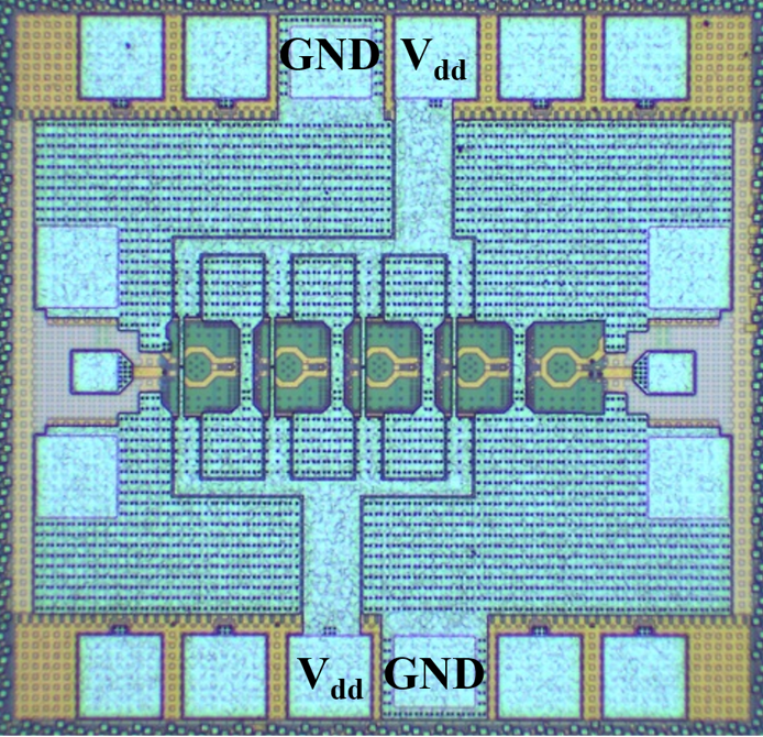
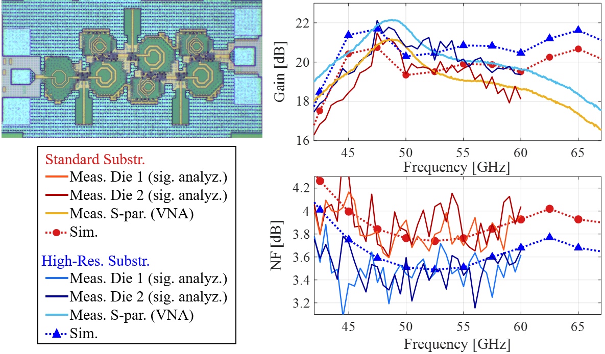
Three-stage 42-67 GHz LNA in 22 nm FD-SOI on Standard and High-Resistivity Substrates
Our paper [60GHzLNA24] describes the design and implementation of a 42-67 GHz LNA using GlobalFoundries’ 22 nm FD-SOI technology, that was fabricated on standard-resistivity as well as on high-resistivity substrate wafers. On the conventional standard-resistivity substrate, the proposed design achieves 3.8 dB of minimal noise-figure for a peak gain of 21.0 dB at its nominal bias under 13.7 mW of power-consumption. The LNA makes use of the unique back-gate bias node of the 22FDX® technology to offer 10 dB of gain-control over a 2 V bias range at the back-gates, and takes up an area of 0.17 mm². On the high-resistivity silicon substrate, improvements of 0.9 dB in gain and 0.4 dB in noise-figure are achieved for this LNA, and these improvements are attributed to the increased quality factors of the integrated spiral inductors present in the design.
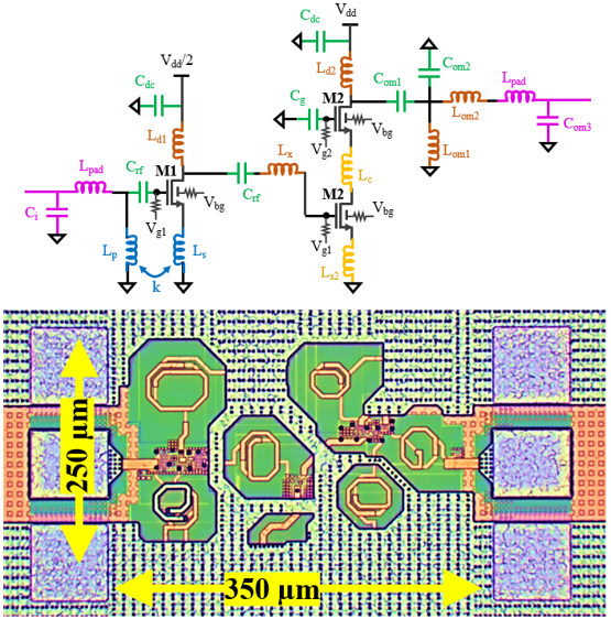
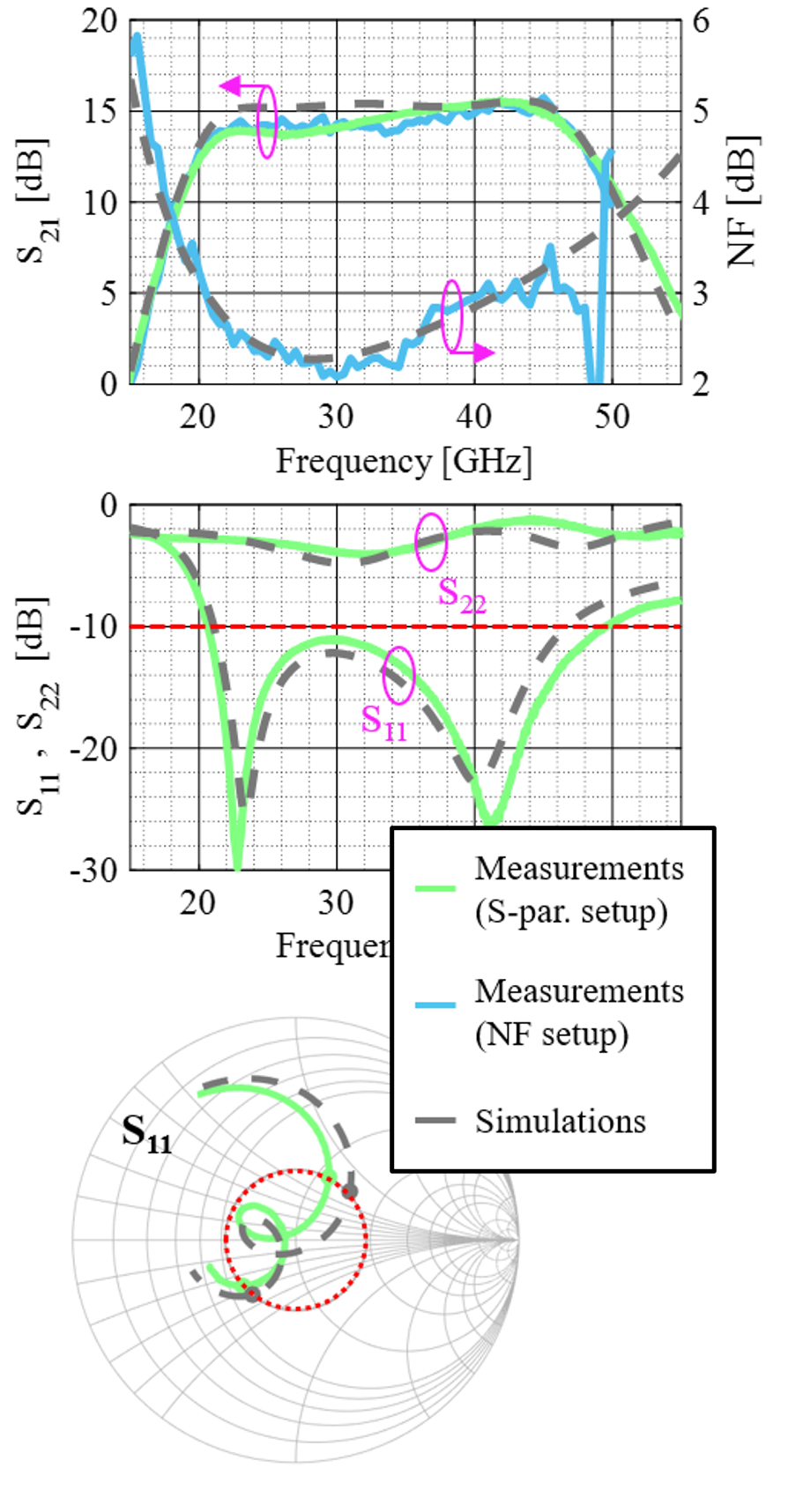
K- and Ka- Wideband LNA in 22 nm FD-SOI with Trasnformer-Tuned Input
Our work [WidebandLNA25] presents a wideband two-stage low-noise amplifier (LNA) covering continuously from 21 GHz up to 47 GHz. The design employs a feedback technique using a transformer-based network at the input common-source stage which introduces poles and manipulates Гopt (by modifying the noise correlations between the input and output), allowing for an eased implementation of simultaneous power- and noise-match over a wide band. The design was fabricated in the low power 22 nm FD-SOI node from GlobalFoundries. At nominal bias, the measured LNA achieves a gain of 15.5 dB over the entire K- and Ka-bands with 2-dB-ripple, and a minimum noise figure of 2.2 dB for 9.1 mW of power. The bias point can also be effectively modulated through the use of back-gate biasing, allowing overall for more than 10 dB of gain-control.
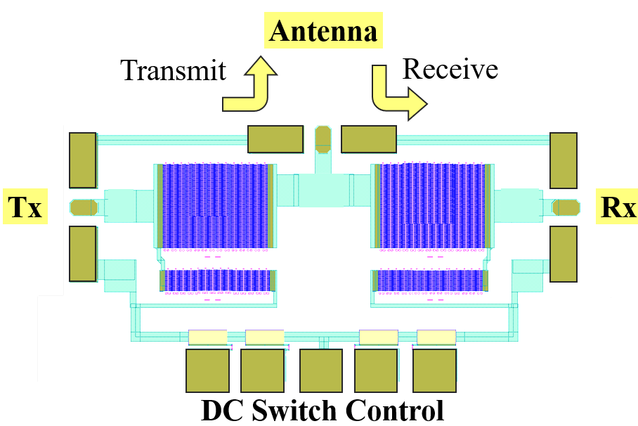
Switch Modules
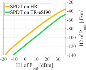
DC-5 GHz SPDT on HR and TR SOI substrates
In the work [RFSW-Sub18], we implemented an RF SPDT switch on two types of RF-SOI substrates: a High-Resistivity (HR) wafer and a Trap-Rich (TR) wafer. The 180 nm partially-depleted SOI node from TowerJazz was used.
Linearity measurements showed that the substrate choice impacts the harmonic distortion of the switch module by more than 15 dB. For these reasons, TR substrates sold by Soitec are named “eSI™”, which stands for enhanced Signal Integrity.
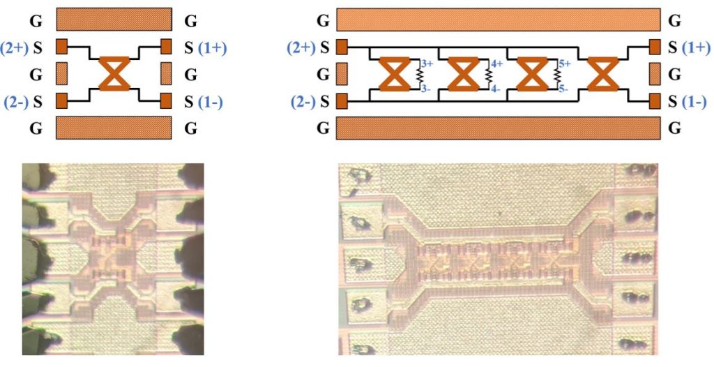
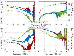
mm-Wave Differential Switch Designs Based on Wave-Cancelling to achieve Ultra-High Isolation
In our paper [DiffSW21], fully-differential SPST and SP4T switches are designed with wideband operation (DC up to 50 GHz) using GlobalFoundries’ 22FDX® platform. Based on a differential modeblocking topology, the switches can achieve isolations better than 50 dB. At 28 GHz, the balanced topology achieves an insertion loss of 1.92 dB, a 1-dB compression of 23.5 dBm and an IIP3 of 47.6 dBm.
DC-40 GHz SPDT in 22nm FD-SOI with Back-Gate
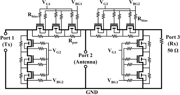
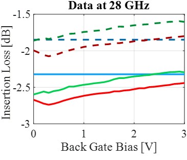
In the work [BG-SPDT20], three ultra-wideband SPDTs fabricated in the 22 nm FD-SOI, each using a different type of millimeter-wave NFET, namely a conventional-well regular-Vt (RVT) device, a flipped-well super-low-Vt (SLVT) device and a specially treated device without back-gate well contact for decreased substrate parasitics (BFMOAT device). It is shown that using the back-gate achieves lower losses, higher isolation and better linearity for the RVT and SLVT based switches, while the reduced shunt-parasitic BFMOAT switch shows better performance at the high-end of the mm-wave spectrum.
Engineering of Shunt-Loss towards DC-120 GHz SPDT Switches in 22 nm FD-SOI
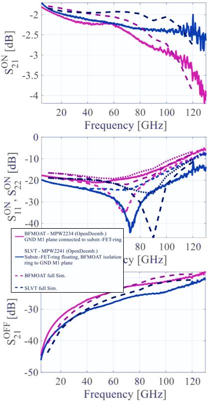
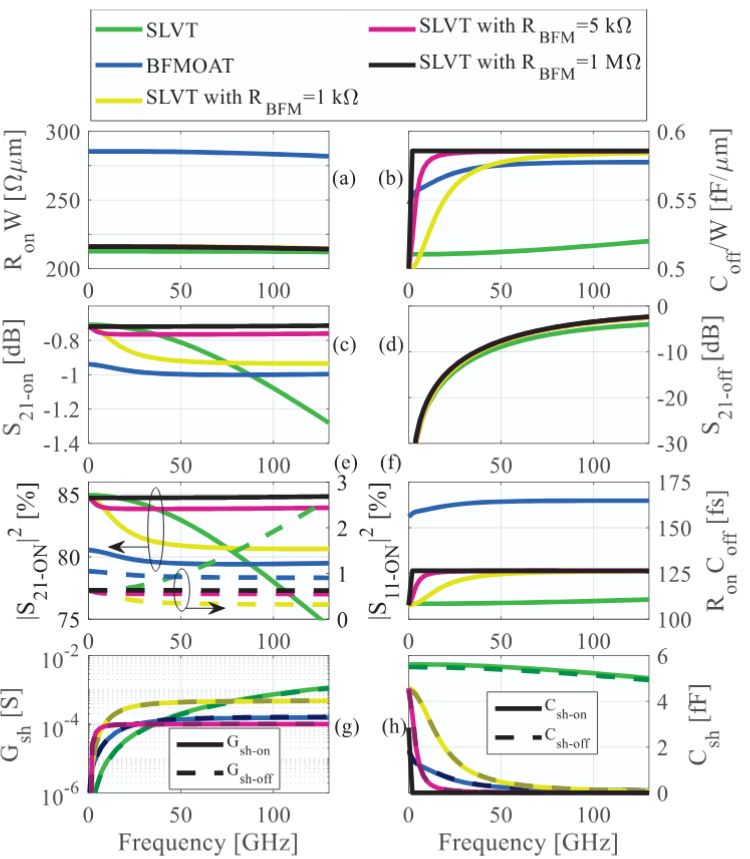
In our works [SwShuntLoss21] and [SwSuntLoss22], wideband SPDT switch designs are explored targeting more than 100 GHz of bandwidth in 22 nm FD-SOI. The effect of shunt loss is studied, since for mm-wave switch applications, the 22FDX® technology offers BFMOAT devices that include substrate isolation zones beneath them to reduce high-frequency shunt loss. However, compared to SLVT devices, this sacrifices the back-gate functionality, resulting in higher RonCoff. This paper proposes and analyses substrate isolation zones implemented in ring-shapes around SLVT-FETs to reduce parasitic shunt admittance while preserving the back-gate. The resulting effective device boasts a low RonCoff metric (thanks to an SLVT-FET core with back-gate) and simultaneously achieves high substrate impedance to the reference ground node (similar performance as BFMOAT-FETs). From such devices, a full SPDT switch was fabricated and characterized up to 130 GHz. Having less than 2.4 dB insertion loss and better than 22 dB isolation from DC to 120 GHz, it outperforms analogous SPDT modules implemented using conventional SLVT or BFMOAT FETs.
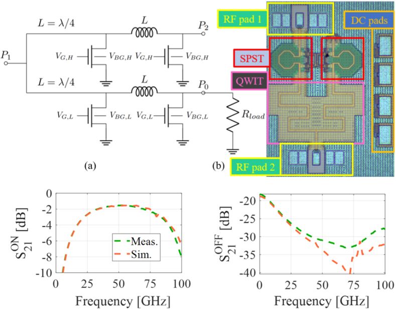
Travelling-Wave Switch Designs in 22 nm FD-SOI at 60 GHz
Our paper [Sw60GHz23] presents 60 GHz travelling-wave SPST and SPDT switch designs in the 22 nm FD-SOI. The full SPDT is composed of a Quarter-Wavelength Impedance Transformer (QWIT) and two SPST cores also fabricated as a standalone devices. The paper details a comprehensive design procedure of the SPST branches and presents the on-wafer measurement data. The losses associated to the QWIT and SPST cores are analyzed in detail and correlated to the performance of the full SPDT design based upon those elements. At 60 GHz, the full SPDT module presents an isolation of 32 dB and an insertion loss of 1.6 dB. Through our dedicated measurement test structures, we identify the various contributing factors to that overall loss, loss induced by the QWIT, by both the transmitting and isolating SPST cores, and by the spiral inductors and FD-SOI devices they are based on.
Power Amplifiers
Dual-Band (28 & 39 GHz) PA - Analysis of Back-Gate Bias on EVM Performance
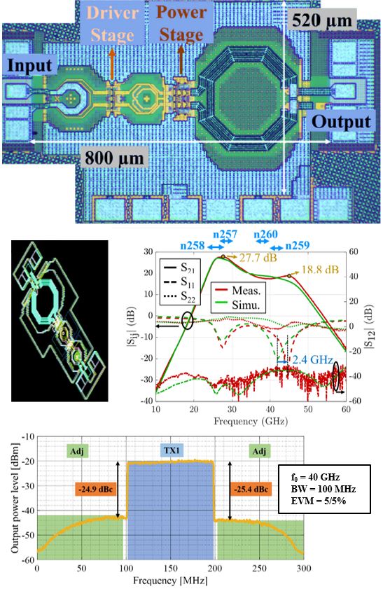
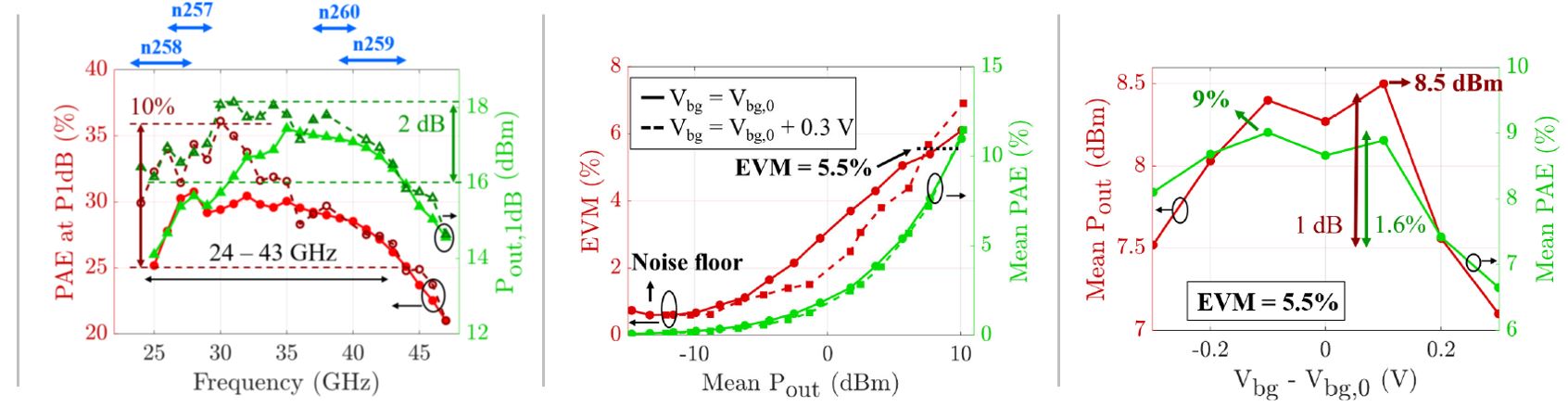
Our paper [PABG25] presents a dual-band power amplifier (PA) covering the 5G n257 to n260 frequency 2 bands (24.25 to 29.5 GHz and 37 to 43.5 GHz), fabricated in 22 nm FD-SOI. Its design is based on a distributed balun at the output that efficiently performs a wideband load impedance transformation. The back-gate terminal of each transistor is connected to different pads for detailed back-gate bias variation analysis. Under 5G new radio (NR) modulated signal measurements, we show how the average output power and efficiency can be optimized by varying the back-gate bias, which optimal value depends on (i) the signal bandwidth, (ii) the carrier frequency and (iii) the target error-vector-magnitude (EVM) value. The impact of back-gate bias control on the system-level EVM figure of merit is studied. Overall, with 7.5 dBm and 7.3% mean output power and efficiency, respectively, at 27 GHz, 6 dBm and 5% at 40 GHz, for a 800 MHz bandwidth 5G NR signal, the designed PA shows outstanding performance among wideband/multiband FD-SOI-based PAs covering the 28 and 39 GHz bands, featuring comparable performance to best-in-class narrowband PA designs in FD-SOI technology.
Voltage-Controlled Oscillators
14 GHz VCO in 28 m FD-SOI - Noise Coupling Mitigation using High-Resistivity Substrate
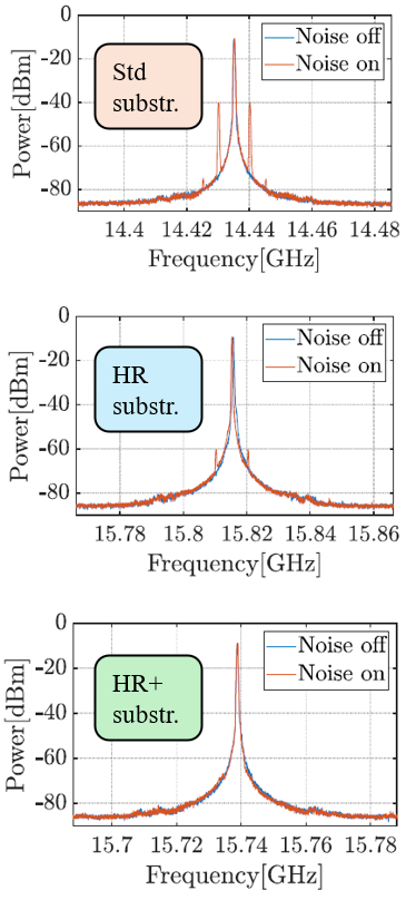
Our paper [VCOsubNoise24] investigates the effect of silicon substrate resistivity on substrate noise coupling and how higher resistivity substrates improve the spectral purity of voltage-controlled oscillators (VCOs). Three VCOs were designed in the 28 nm fully depleted Silicon-on-Insulator (FD-SOI) technology and implemented on process-of-reference (POR) wafers (10 Ω.cm) as well as high-resistivity (HR) wafers (1 kΩ.cm). The output spectrum of the VCOs is measured with and without the injection of a 0 dBm noise signal into the substrate. Results show the highest reduction in the parasitic spurs caused by the noise signal to be more than 26 dBs when using a passivated HR substrate. To the best of the author’s knowledge, this is the first time VCOs are fabricated and measured on HR substrates in FD-SOI technology to explore their effectiveness in the reduction of substrate noise coupling.
Mixers
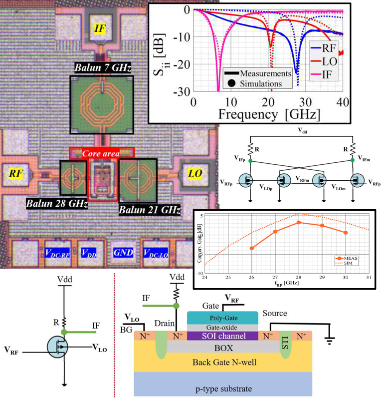
28 GHz Down-Conversion Mixer Employing a 22 nm FD-SOI FET as a Dual-Gate Device
Our paper [MixBG22] presents a novel 28 GHz down-conversion mixer topology using the back-gate terminal in 22 nm FD-SOI as an RF excitation port for the 21 GHz local oscillator (LO) signal. A double balanced architecture with an active load and transimpedance amplifier were implemented in the 22FDX® technology from GlobalFoundries. The mixing functionality is provided at the level of a single FET, that is simultaneously excited at the front- and back-gates by the RF and LO signals, respectively. Under 0.9 V power supply (26 mW DC consumption) the proposed down-conversion mixer exhibits a maximum conversion gain of 3.5 dB by applying 10 dBm of LO power. The 1 dB compression point occurs at -6 dBm of RF input power and the third order intercept (IIP3) point is 15 dBm at nominal LO power. Benchmarking these values against mixer performances from the literature reveals this design to be close to the current state-of-the-art in CMOS and SOI technology, demonstrating the viability of this novel topology employing back-gate excitation at mm-wave frequencies.
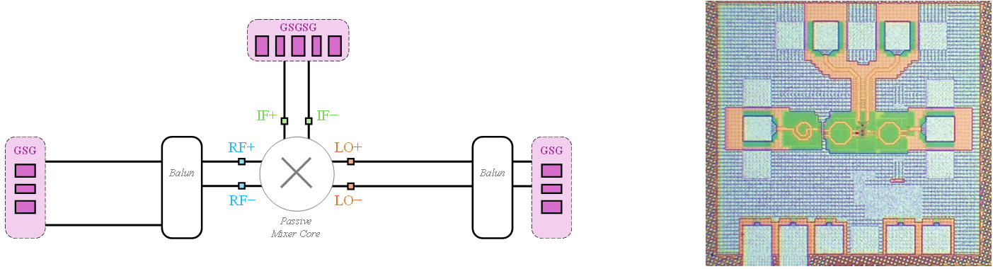
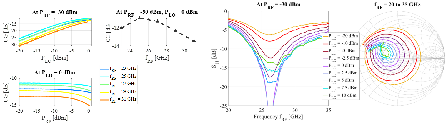
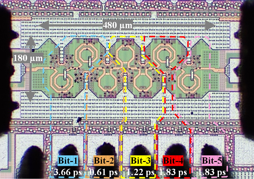
Wideband 23-31 GHz Passive Down-Conversion Mixer in 22 nm FD-SOI
Publication pending.
More information on this design will be shared in the near future.
Phase-Shifters
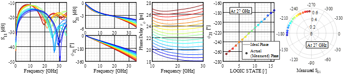
DC-30 GHz Phase-Shifter in 22 nm FD-SOI with True-Time Delay Characteristics
Publication pending.
More information on this design will be shared in the near future.
Power Detectors
D-Band Power Detector Designs
Results pending.
Receiver Chain
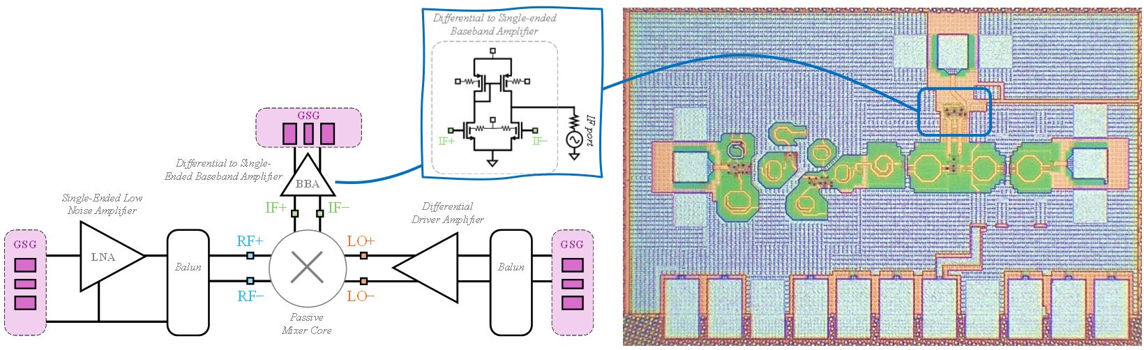
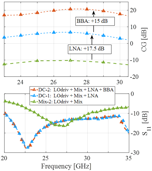
Wideband 23-31 GHz RX-Chain with LNA, Down-Conversion Mixer and Baseband Amplifier in 22 nm FD-SOI
Publication pending. A down-converter receiver chain covering from 23 to 31 GHz was designed, fabricated and measured using 22 nm FD-SOI technology. It includes a wideband LNA at its input, followed by a wideband passive mixer. The passive mixer in driven by an on-chip LO amplifier, and at the low-frequency output a baseband amplifier (BBA) is incorporated to further increase the gain.