Infrastructure
& Expertise
UCLouvain's "WELCOME" Platform
Characterization Tools
WELCOME facility is the Wallonia ELectronics and COmmunications MEasurements platform at UCLouvain (website, virtual tour).
It provides state-of-the-art multidisciplinary technological tools in the field of electrical and electromagnetic characterization, enabling measurements ranging from the physical behavior of materials, sensors and devices, to the behavior of complex system architectures and wireless signal propagation.
A powerful range of equipment and an exceptional pool of expertise acquired over more than 40 years at UCLouvain are available to support various research axes including micro- and nanotechnology (materials and devices), Silicon-on-Insulator technology, RF and microwave circuits, digital systems and VLSI architectures, MEMS/NEMS, cryptography, ultra low-power wireless biometric and biological sensors, molecular electronics, signal propagation and wireless communications between sensors.
The infrastructure goes further bringing together three pillars: research, education, and services to the industry. WELCOME helps to cover all steps of development in electronics and communications, from design to prototyping, including modeling, fabrication, testing and reliability assessment.
Characterization and Extraction
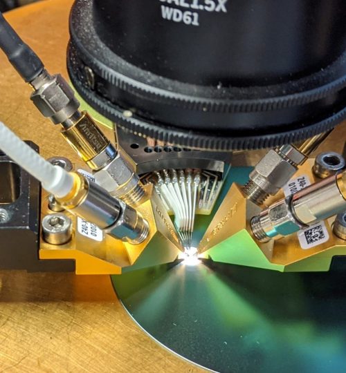
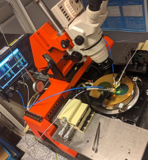
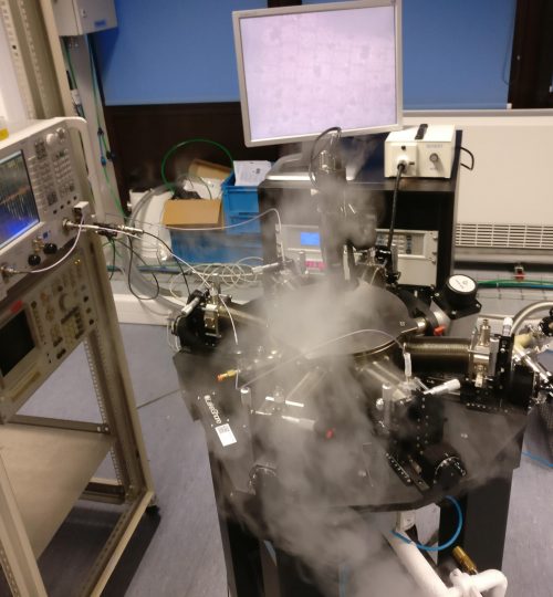
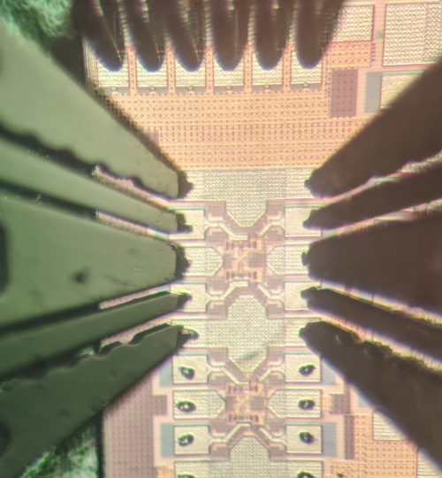
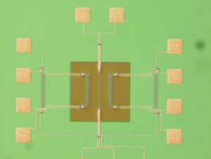
UCLouvain’s RF-SOI group have developed test-benches as a part of WELCOME for extensive on-wafer device and RF characterization, including:
- Ultra-wideband VNA characterization from 900 Hz to 130 GHz.
- Large-signal measurements up to 30 dBm over a range of fundamental frequencies (between 50 MHz and 28 GHz).
- Chuck temperatures from 4 K to 200°C.
incize is a spin-off company from UCLouvain’s RF-SOI research group that specializes in particular in state-of-the-art on-wafer device characterization.
Visit incize‘s website for more information.
Fabrication Tools
UCLouvain's "Winfab" Cleanrooms
Winfab is the Wallonia infractructure nano-fabrication platform at UCLouvain (website).
1000 m2 of cleanroom is spread over two levels, with over 50 high-tech equipments fleet thatand offer a wide range of advanced micro- and nona-fabrication techniques.
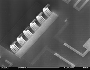
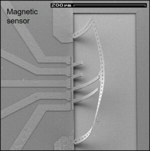

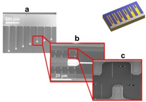
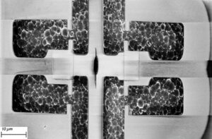
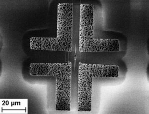
Winfab is a multidisciplinary platform active in various research and technological fields, including SOI (silicon-on-insulator) CMOS microelectronics, microelectromechanical systems (MEMS), lab-on-chip devices, sensors, solar cells, batteries, bio-technologies, nanoelectronics, 2D materials (graphene, …), photonics devices, organic electronics, and more.
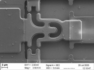
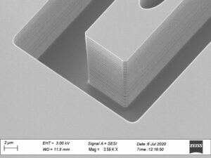
RF Substrate Development
In particular, the Winfab platform has served over the years to develop novel RF substrate solutions:
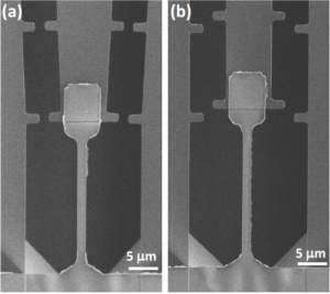
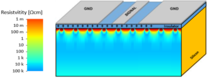
- Starting with trap-rich-passivated high-resistivity substrates in the early 2000’s [DL05p, DL05], this solution, developed in UCLouvain’s Winfab facilities, is nowadays the reference substrate solution for RF applications, being commercialized by Soitec as the RFeSI™ (RF enhanced Signal Integrity) products [1, 2, 3].
- UCLouvain has also been developing porous silicon as an RF substrate solution for several years. Starting with a frontside porosification approach using highly-doped silicon wafer [YB14, YB17], the process was successfully applied to standard resistivity samples in [MR18]. In 2019/2020, a post-CMOS-process approach was proposed, by which localized porous regions are formed after the foundry process, in targeted areas for increased RF performance, and initial Winfab-fabricated prototype results demonstrate excellent performance in [GS19i, GS19ss].
- A novel interface passivation scheme was proposed in 2019 to counter the parasitic surface conduction effect in high-resistivity silicon wafers (similar objective as trap-rich passivation) by employing a smart array of P- and N-doped regions at the interface. Initial prototypes fabricated in Winfab showed promising performance results in [MR19], and implementations at the industrial level further demonstrate the achievable passivation quality in a full foundry process [MM21, MR22, LN22, MR24].
Simulation Tools
Simulation and Modelling Capabilities
UCLouvain has expertise in simulation and modelling ranging from TCAD-type semiconductor physical and electrical modelling to electromagnetic simulations of propagating waves up to the high mm-wave frequencies.
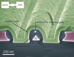
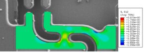
Semiconductor Physics (TCAD)
UCLouvain has expertise in TCAD device simulations at the transistor and at the substrate levels.
Using TCAD suites such as Silvaco (Atlas, Athena, Victory) or Synopsys (Sentaurus), the UCLouvain’s RF-SOI group has simulated and modelled various effects, notably:
- Substrtate loss effects due to a parasitic surface conduction layer induced by fixed positive interface oxide charges [DL05, MR19e], and ways to counter it, including the TCAD modelling of trap-rich [MR21a, MR21b], Au-compensated silicon [MN19], and smart PN interface implants [MR19].
- The impact of the source/drain underlap charge on channel mobility extraction in short gate-length devices (28 nm FD-SOI) [AM21].
- The substrate’s effect on the output conductance’s (gd) signature over frequency [VK02], and its impact on the extraction of self-heating characteristics of FD-SOI devices [LN21, MV21].
- 3D simulations of sub-100 nm multi-gate devices [TM06].
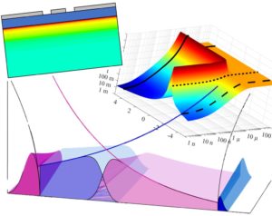
- The non-linear behavior of silicon-based substrates at RF, and the evaluation of signal distortion. In [MR21a] physical mechanisms are highlighted, including carrier and trap finite response times, and in [MR21b] extensive model-hardware correlations are presented.
Electromagnetic Simulations (EM)
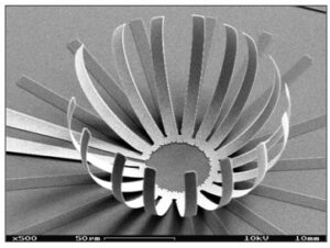
UCLouvain regularly performs EM simulations, that solve for Maxwell’s equations, typically in RF and mm-wave passive devices and interconnects such as spiral inductors, transformers, baluns, and transmission lines.
The following EM tools are regularly used at UCLouvain, in particular for the following applications:
- Momentum from Keysight is used as either a standalone solver in the ADS environment, or as a plugin EM solver in the Cadence environment (of a foundry PDK) to rapidly and accurately compute EM interactions in metallic back-end-of-lines.
- HFSS from Ansys and CST Studio Suite from Simulia are employed as a 3D field solvers to model a variety of EM effects, including multi-mode excitations in waveguides [4] and parasitic modes originating from probe-to-chip or probe-to-chuck coupling at high-end mm-wave frequencies [5, 6, 7].
- In particular,our works [LD1, LD2] on high-frequency on chip antennas study the effects of surface waves on their energy efficiency. In [LD1] we propose a method of capturing and radiating the generated surface waves, making the antenna’s radiation pattern independent of edge effect and chip dimensions, while in [LD2] we extend the study to different properties of the Si-substrate, from standard resistivity materials to high-resistivity and trap-rich substrates.
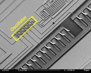
RF-IC Design
Cadence Virtuoso software is employed at UCLouvain to run the PDK models of a variety of foundries, and in particular advanced SOI nodes targeting RF and mm-wave applications.
From a simulation and modelling perspective, this includes:
- Running the DC and RF testbenches in the ADE tool of active devices, netlists, S-parameter files, and more.
- Using Momentum from Keysight to generate interaction matrices of the full fabricated layout and passive components, usually running on the top metal layers of the BEOL.
- Running parasitic extraction tools to model the added resistive and capacitive networks around active devices, usually accounting for the impact of interconnection in the lower-level metals of the BEOL.
- Verifying fabrication design rules (DRCs) as well as DC and RF current density design rules and failure rates (electromigration).
- Controlling metal dummy fill densities for reduced (and known) impact on RF passive behavior.
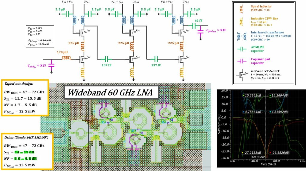
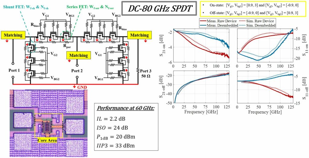
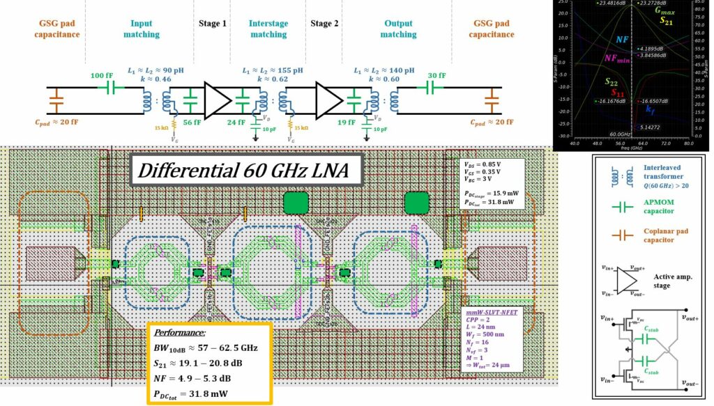
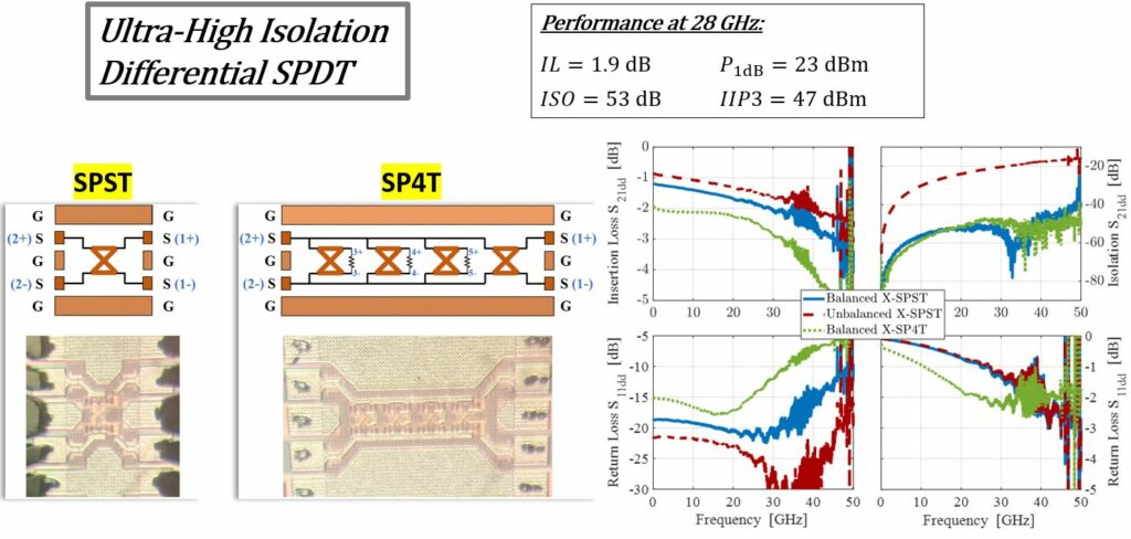
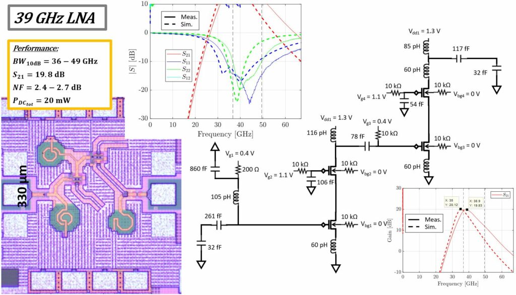
UClouvain’s RF-SOI group has demonstrated excellent hardware-simulations agreement for a variety of RF and mm-wave circuits. Please consult our dedicated page on RFIC designs for more details.
Multiphysics
UCLouvain’s team also has experience in multiphysics simulations, such as:
- The non-linear behavior of silicon-based substrates at RF, and the evaluation of signal distortion. Distributed electromagnetic effects must be taken into account when simulating RF passives, but to capture the non-linear field-sensitivity of the electrical properties of semiconductor substraters, these must be coupled with semiconductor transport equations and physics. UCLouvain have developed such a modelling approach. Physical mechanisms are highlighted in [MR21a], including carrier and trap finite response times, and in [MR21b] extensive model-hardware correlations are presented.
- Using commercially available multiphysics tools (such as Comsol Multiphysics from Comsol or OOFELIE Multiphysics Suite from Open Engineering) to model a variety of effects, such as:
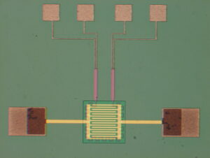
- Micro-Electro-Mechanical Systems (MEMS) for RF switch applications.
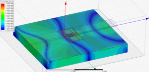
- Heat propagation and dissipation within a chip, originating from the self-heating effects of active devices.
- Surface Acoustic Wave (SAW) filters for RF application on piezoelectric materials.